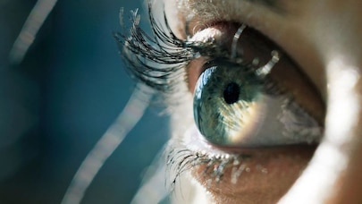
The charge-coupled device CCD provided the first way for a light-sensitive silicon chip to store an image and then digitize it, opening the door to the creation of digital images
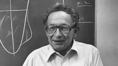
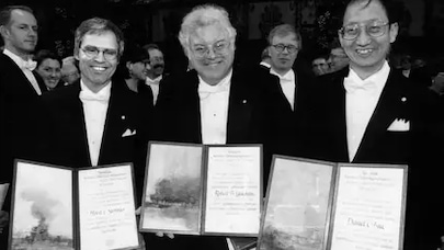
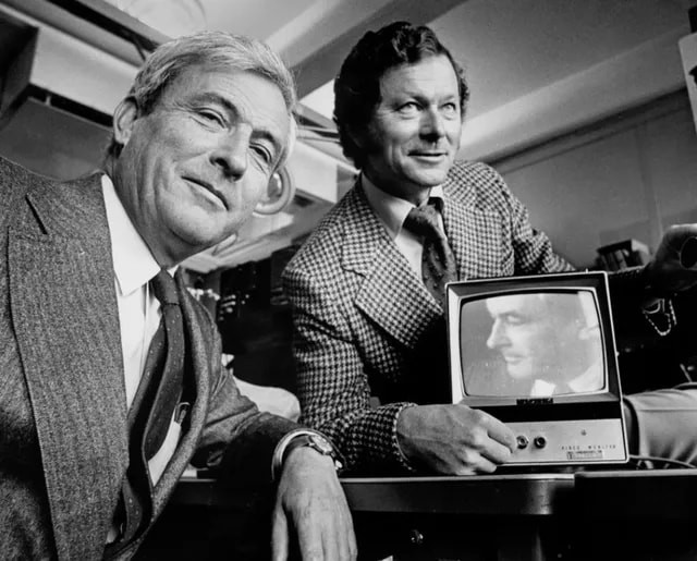
The 2009 Nobel Prize in Physics was awarded for two scientific achievements that helped to shape the foundations of today’s networked societies. Willard S Boyle and George E Smith of Bell Labs were awarded the prize “for the invention of an imaging semiconductor circuit—the CCD sensor.”
Boyle and Smith shared the prize with Charles K. Kao for his “groundbreaking achievements concerning the transmission of light in fibers for optical communication.” Leveraging the photoelectric effect, by which light is transformed into electric signals, the CCD provided the first practical way to let a light-sensitive silicon chip store an image and then digitize it.
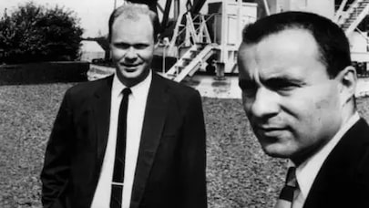
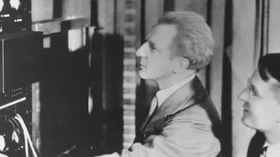
Boyle and Smith came up with the idea for the CCD in October of 1969, sketching out the basic design, principles of operation, and preliminary thoughts about applications during a brainstorming session that lasted less than an hour. The two were working on semiconductor integrated circuits, and Smith had been involved with trying to create an imaging chip for the Picturephone, which consisted of an array of silicon diodes. At the time, Bell Labs was also working on a new type of computer memory that relied on tiny bubbles of magnetism. Upper management was anxious to speed up the development of magnetic bubbles as a major memory technology, and the pair was encouraged to come up with a compelling semiconductor device or potentially risk losing funding.
Boyle credited Bell Labs brainstorming sessions for inspiring the CCD. He and Smith came up with the idea at a blackboard and immediately “knew we had something special.”
To create a CCD, a layer of silicon is doped so that it is deficient in electrons and oxidized at the surface. An array of metal electrodes is added on top of the oxide to form gates, creating capacitors that can store charge. Voltage is then applied to the gate, which repels the silicon’s positive carriers—the holes—and creates a potential well at the silicon’s surface. When a photon strikes the silicon, it creates an electron–hole pair, and the electron moves toward an electrode into the well. Electrons accumulate in the interface between the silicon and the oxide. When a sequence of high and low voltages is applied to adjacent gates, the electrons shift from one gate to the next until they reach the edge of the chip, where the level of charge can be read as a measure of light intensity.
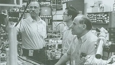
The CCD has revolutionized photography, allowing light to be captured electronically instead of on film. Imaging device applications of CCDs are found in digital cameras, TV cameras, scanners, medical devices, fax machines, bar code readers and surveillance technologies. Among the most impressive scientific applications were in astronomy, where the advantages over using photographic film led to many new discoveries.
References
- http://www.nobelprize.org/nobel_prizes/physics/laureates/2009/press.html
- http://journals.aps.org/rmp/pdf/10.1103/RevModPhys.82.2305
- http://journals.aps.org/rmp/pdf/10.1103/RevModPhys.82.2307
- http://ieeexplore.ieee.org/xpl/articleDetails.jsp?arnumber=1478484
- http://spectrum.ieee.org/consumer-electronics/gadgets/nobel-goes-to-boyle-and-smith-for-ccd-camera-chip
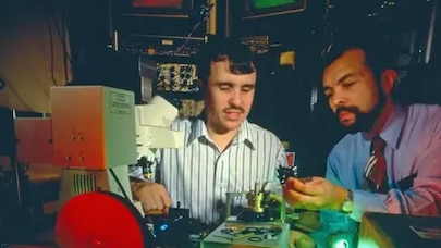
Michael Tompsett applied the Charge-Coupled DeviceCCD specifically to imaging application and, along with his team, developed a series of CCD Ccameras. The photo above, is the first color pixel image, probably of his Tompsett’s wife.