How “growing” optical lasers will change the way we build fiber networks
The ever-growing demand for data capacity has triggered a revolution in optical communication. Fiber is rapidly making its way into more places and more end devices. Meanwhile fiber technologies are growing more complex as we develop more sophisticated ways to transmit information over light. Our current methods of manufacturing optical devices can’t keep up with those two competing demands.
We need to find new and cheaper ways of manufacturing more-efficient and higher-performance optical modules to power the fiber networks of the future. One of the most intriguing solutions to this problem is to move away from today’s methods of building optical modules from separate components and look toward the semiconductor industry for inspiration. Instead of “assembling” optical modules, we can “grow” them.
Silicon and light don’t mix
Currently the optical modules that transport the world’s data consist of two distinct components: a laser source and a chip connected to that emitter via a fiber. Both components are manufactured separately using vastly different methods, then later assembled. The chip is made from silicon using the same high-volume, low-cost fabrication techniques utilized by the microelectronics industry. Meanwhile, the laser source is fabricated from alloys made from indium, gallium, aluminum, arsenic and phosphorus. These alloys are known to chemists as III-V materials due to the location of their component elements on the periodic table.
These III-V alloys have unprecedented properties when it comes to emitting light, making them ideal for any fiber-optic system. However, the fabrication process for these materials is expensive, and they can only be produced in small volumes -- in stark contrast to silicon chips. That creates a fundamental scalability roadblock. We are essentially taking an easily manufactured, cheap component and pairing it with a hard-to-manufacture, costly component every time we build a single optical module.
The seemingly obvious solution is to use a single fabrication process to integrate the laser source with the chip. But that’s easier said than done. Light can’t be generated from silicon, so a single optical module made entirely from silicon isn’t possible. We’ve explored bonding III-V materials directly onto a silicon wafer, but that kind of integration is difficult. The process is complex and less cost-effective than the current methods of assembling an optical module out of separate components.
This problem has perplexed the telecom industry for 30 years, but we may finally have a solution that could bring these two families of materials together on a single chip.
Growing lasers in a silicon garden
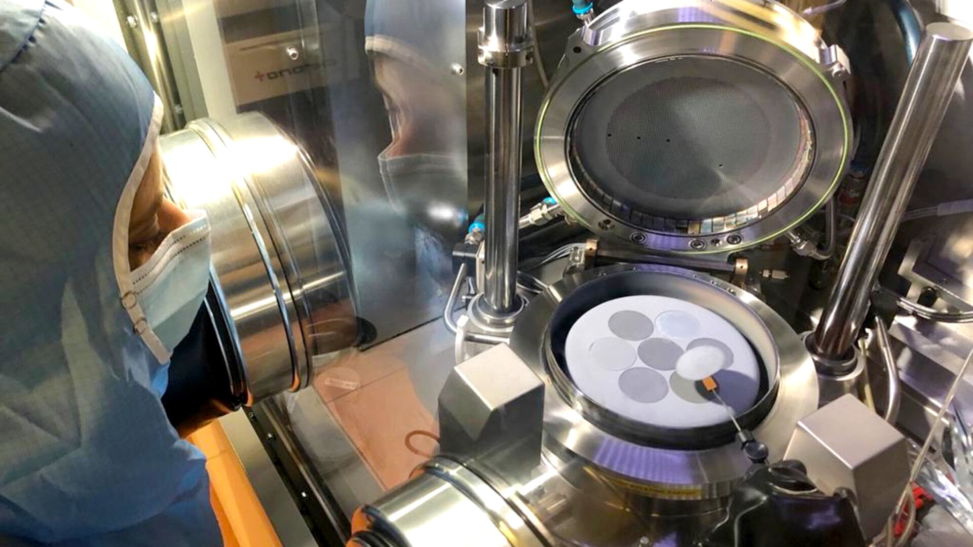
To create a high-performance, cost-efficient optical module, we need to grow the laser source directly on the chip. Normally this would be a near impossible task because most III-V elements are incompatible with silicon. Nokia Bell Labs, however, has developed a method for layering III-V materials onto a silicon wafer. We start by bonding an unprocessed film of indium phosphide onto a large silicon wafer. Then, on that film we begin growing III-V alloys that will become the laser source. We would no longer need to assemble optical modules from two components. We would merely grow one component on top of the other.
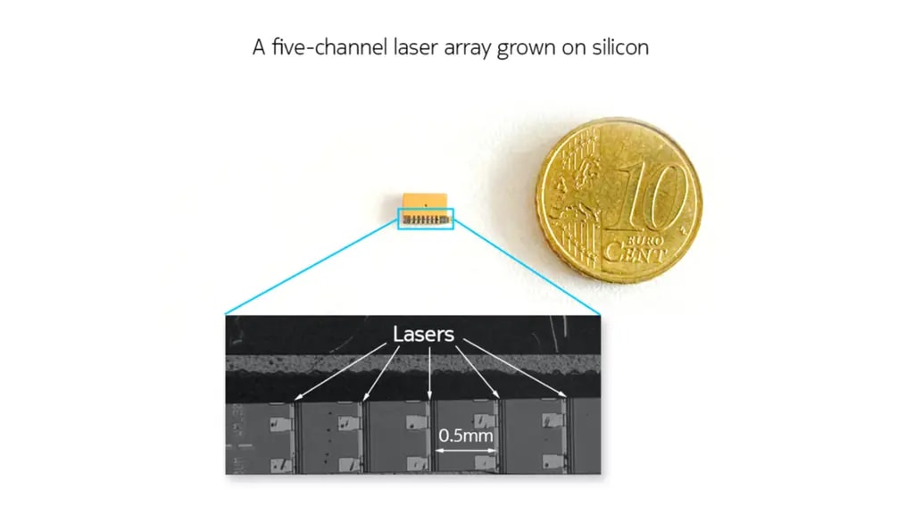
In 2020, Nokia Bell Labs successfully grew a five-channel laser array emitting at five different wavelengths covering a 155-nm-wide spectral range over silicon. This is significant because we were able to show that our bonding-and-growth method could create a high density of high-performance components, which are needed in optical system to maximize bandwidth. Today’s optical module manufacturing methods would require fabricating five different lasers made from five different alloys from five growth steps and then assembling them. The III-V Lab in Paris-Saclay was able to grow this dense laser array with a single growth step on a large silicon wafer.
This approach meets all the competing requirements of optical networks going forward. The manufacturing process is much less complex and expensive than today’s methods as it follows the model of the microelectronics industry. But cost isn’t the only benefit. An integrated module is also a higher-performance module. Placing the laser source directly on the chip suppresses lossy optical couplings that limit the overall performance of the system, meaning we’ll get more-efficient, higher-capacity optical systems. It also allows us to manufacture smaller devices.
This bonding-and-growth method is also highly versatile since the generic bonding film we use offers the possibility of growing any kind of photonic component, from amplifiers to modulators, which will in turn produce higher-density and higher-performance optical systems. Last, but not least, by integrating these components, we no longer need to provide separate cooling systems for them, thus lowering power consumption.
Myriad possibilities for silicon photonics
Though we’re excited about the possibilities for integrated modules, there are still some obstacles to overcome before we can start growing optical components onto silicon commercially. There aren’t many semiconductor plants today that specialize in silicon photonics. That means the industry will need to invest in the infrastructure that would make integrated optical modules a reality.
There will likely be plenty of incentive, however, for the industry to pursue new means of manufacturing optical systems. We are laying fiber to homes and businesses at a dizzying rate. Optical interconnects are becoming the glue between edge data centers. Our cellular networks are becoming webs of fiber backhaul and fronthaul connections. Those trends will demand more cost-efficient optical equipment. Meanwhile, the move to more sophisticated multimode and multicore systems will demand higher-performance components.
And while the initial target for this technology will be fiber-optics, silicon photonics can be applied to numerous other industries. We could grow photosensors for the imaging industry or photovoltaic cells for the solar-energy industry. We can even address LiDAR applications. Decades ago, a process called complementary metal-oxide-semiconductor, or CMOS, revolutionized the semiconductor industry, opening up previously unimaginable possibilities in microelectronics. We believe silicon photonics with fully integrated lasers and detectors could revolutionize the optical industry in the same way.