Putting light on a chip: How lasers will advance quantum computing, neural networks and more
What do quantum computing and optical networking have in common? The photon.
That’s right, the most elementary particle of light could one day make quantum computers’ most sophisticated calculations. And they would do so by tapping into the same technologies that power the vast fiber-optic networks that encircle the earth.
One of the exciting new areas of research is in optical quantum computing, which uses photons to represent the quantum bit, or qubit, the most basic unit of information in quantum computation. Unlike an ordinary bit, which can only store one of two values, a 0 or a 1, the qubit can store multiple values simultaneously. By combining many photon qubits together, optical quantum computers are expected to greatly enhance computational power, putting the number-crunching skills of today’s classical computers to shame.
This is where optical networking comes into the picture. The same lasers we use to generate the wavelengths of light that carry information across the globe through fiber could generate the qubits used by future optical quantum computers, as well as provide other key components for all quantum computers. What’s needed is a way of incorporating those lasers and detectors directly into electronic components. Silicon photonics technology uses low-cost fabrication and mature micro-electronics technology to guide and control light. As such, it is an excellent compact photonic platform to route optical signals on a chip. However, silicon as an optical medium in Silicon Photonics platforms does not generate or detect light efficiently.
At Nokia Bell Labs we are tackling this unique problem head on. Our foundational research in optical networking has led to discoveries that we are now applying to technologies well beyond communications. For that, we are developing new solutions to solve the problem of fusing active optical components onto silicon photonics. One of our areas of expertise is in the use of a special category of semiconductor alloys known as III-V materials, which are named after their location on the periodic table of elements. Through the integration of light sources, modulators and detectors enabled by our mature heterogeneous III-V-on-silicon technologies, Nokia Bell Labs has found ways to use these materials to enhance the functionality of silicon-photonic integrated circuits, effectively reproducing a miniaturized fiber-optic network at the chip scale.
In this blog post, we’re covering some of the potential applications for this research as well as the specific integration techniques our team at Bell Labs is researching that could make those applications a reality.
Needless to say, quantum computing is just the beginning.

From III-V crystals to neural networks
We see much potential in AI neural networking exploiting such heterogeneously integrated silicon photonic platforms. Neural networks generate synaptic signals between nodes, or “neurons,” in a way that emulates neural activity in the human brain. Typically, these synaptic signals are generated electrically. But if we were to use integrated lasers/modulators and detectors on silicon photonic chips that emulate brain-inspired synaptic architectures, then we could potentially boost neural networks’ already impressive computational power.
All these high-tech applications rely on the density of integration of such III-V lasers, modulators and detectors on a tiny photonic chip. The oldest way of integrating active optical components on silicon is the hybrid integration based on the manufacturing of III-V semiconductors and silicon photonic chip separately. Then, the light coupling is made by carefully placing the III-V chip side by side with the silicon chip. This cumbersome approach cannot be used to produce integrated lasers in high volumes and suffers from optical losses.
To increase the density of integration and maximize the optical performance, we rely on the heterogeneous integration that bonds a large patch of III-V semiconductor onto silicon like paste stickers. After fabrication, we obtain arrays of several unitary devices, each about the size of a grain of sand.
Our team is studying other approaches with the aim of pushing the limits of optical performance, optimizing the way such III-V materials are integrated on silicon. For instance, in a previous blog post, our colleague Claire Besançon described Nokia Bell Labs’ cutting-edge research into not bonding but “growing” lasers made of III-V materials directly onto silicon.
Smaller, cheaper and more sustainable
While there are many emerging applications for III-V-based devices on chips, we also apply these same advances to established optical technologies, making them more efficient, less expensive and better performing in the process.
In optical networks, integrating lasers on silicon photonic chips will inject massive performance gains into the long-haul fiber networks that crisscross the globe. Collaborating with CEA-Leti, Nokia Bell Labs has produced integrated lasers that can generate much purer and stable optical beams, hence improving the quality of optical transmissions. Moreover, integrated lasers can be combined with other components to increase data transmission rates. As such, this research will create much higher-performance optical networks while simultaneously minimizing infrastructure costs.
Self-driving cars will also potentially benefit from heterogeneous photonic technologies. Today, Light Detection and Ranging (LiDAR) sensors are used by many autonomous vehicles to scan their surroundings so they can navigate and avoid pedestrians, obstacles and other cars. Developing LiDAR systems at low cost and in a compact form factor will be fundamental to bringing these sensors to a broad range of vehicles. Silicon photonics integration technology is quickly advancing toward LiDAR-on-a-chip technologies that could not only meet these size and cost requirements, but also improve performance as compared with current LiDAR technologies. Integrated lasers can also be designed to transmit in the near-infrared range where they are much safer to the human eye, and they generate much purer optical beams, increasing their localization sensitivity.

Finally, by integrating lasers and detectors onto silicon chips, we cut down on the energy needed to operate laser-based applications and even potentially reduce battery-material costs. Integrated lasers use only a small fraction of the materials that would go into a laser assembled from separate components, making these novel technologies much more sustainable.
One of the most exciting research areas in silicon photonics is in new micro-transfer printing techniques, which replace the bonding step of a large patch of III-V semiconductor with many individual III-V chips. In micro-transfer printing only a thin membrane of material is used to form all the optical components of an integrated III-V device at micro-scale. The optical components are entirely manufactured on the thin III-V platform and only afterwards do we pick and place all of them together in the correct locations on the silicon chip. IMEC and Nokia Bell Labs have demonstrated the feasibility of micro-transfer printing by producing a widely-tunable integrated laser that could have applications not only in telecommunications, but also in optical sensing, spectroscopy and healthcare.
Optical lasers may be the primary means for transferring data around the world, but clearly their potential is even greater. The marriage of III-V-materials techniques and silicon photonics is opening doors for numerous more optical applications from quantum computing and encryption to AI and LiDAR. As the advances we describe here make integrated III-V devices cheaper, smaller and more powerful, that potential will only increase.
For a more detailed look at Nokia Bell Labs research in heterogeneously integrated silicon photonic platforms, micro-transfer printing and other techniques, please read our IEEE Spectrum paper.
Interested in learning more about our Optical research and vision. Check out our Optical communication page.
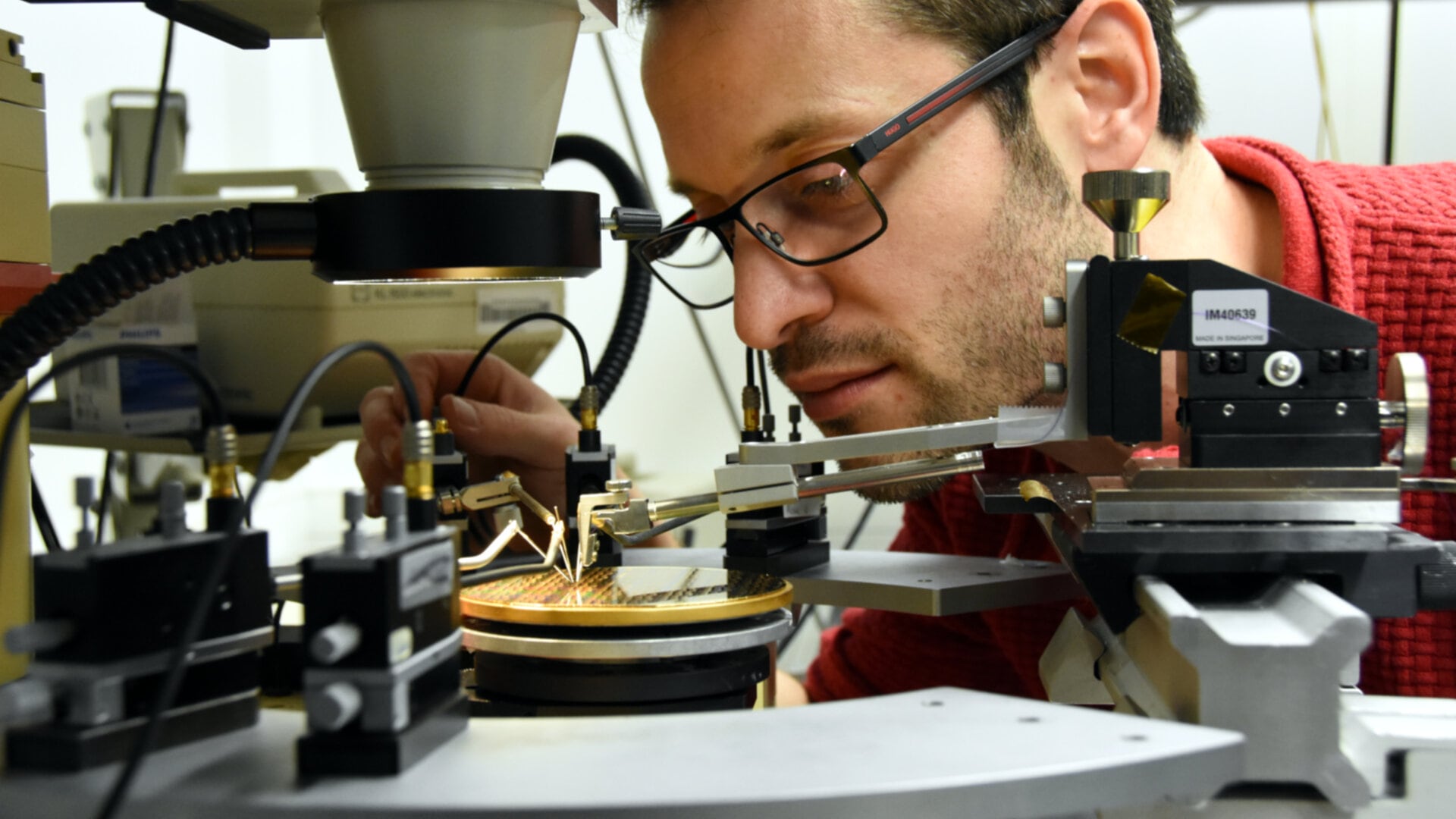
Image captions from top to bottom: 1) Joan Ramirez working with a III-V integrated laser on a silicon wafer, 2) Nicolas Vaissiere working with crystals that will form lasers, 3) an integrated laser array made at the III-V shown at scale

