Silicon photonics: the platform for the 400G era and beyond

The continual advancement of optical and silicon technology has enabled network operators to keep pace with the explosion in video and mobile bandwidth demand over the past decade. However, traditional technologies are approaching fundamental limits of transmission capacity and processing power. Network operators need new ways to scale their networks to meet the surging demands of 5G and the cloud while simultaneously containing cost. They must rethink the way they architect their networks and data centers, right down to the component level.
Silicon photonics is the revolutionary technology that enables the major improvements in performance, density and economics required to enable 400G everywhere, and make next-generation optical communications networks a reality. Nokia’s silicon photonics technology, developed over several product generations, drives the miniaturization and integration of complex optical subsystems into silicon chips, dramatically improving performance, footprint, and power efficiency, while reducing the cost of moving data around data centers and around the world.
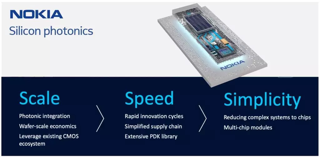
Silicon photonic integrated circuits take scale, speed and simplicity to new levels

Silicon photonics and the importance of integration
Recent generations of optical technology have driven a trend toward pluggable, application-optimized coherent interfaces featuring small form factors. With the latest generation of optics, this trend expands to include digital coherent optics (DCOs) that tightly integrate digital signal processors (DSPs) and optical front end components into small form factor pluggables such as CFP2-DCO or QSFP-DD. These form factors are impossible to realize with traditional discrete optical components, which are prohibitively bulky, power-hungry, and expensive for such applications.
By integrating key discrete photonic components of the optical transceiver into silicon chips, the Nokia silicon photonics platform significantly increases port density, improves performance and power efficiency and simplifies manufacturing as compared to traditional optics technology. All this enables new architectures and applications – including integration into both IP router and optical transport platforms – and helps network operators reduce overall cost per bit.
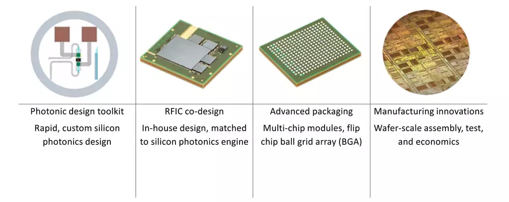
Our proprietary technology includes critical elements from design to volume manufacturing. This includes a state-of-the-art photonic design toolkit, in-house co-designed RFICs, advanced optoelectronic packaging technologies, and rapid wafer level test and characterization capabilities. Leveraging the advanced technical capabilities of existing electronic application-specific integrated circuit (ASIC) fabrication facilities, Nokia is introducing highly integrated photonic devices and achieving high-volume manufacturing quickly. This fosters cost, time-to-market, and complexity scaling advantages that are typically unheard of for emerging technologies.
Key elements for reducing optical subsystems to chips

Using silicon photonics to power new optical applications
Silicon photonics has proven to be a compelling platform for enabling next-generation coherent optical communications and intra-data center interconnects. This technology can support a wide range of applications, from short-reach interconnects to long-haul communications. It has already gained significant market traction in metro, data center interconnect, and intra-data center applications, and is widely viewed as a key enabler for next-generation networks.
Our 3rd generation of silicon photonics solutions includes the Coherent Silicon Transmitter and Receiver (CSTAR) portfolio of optical engines for 100G to 400G coherent applications, which can be designed into both pluggable and on-board form factors. These optical engines offer a highly compact form factor, low-power operation, and unprecedented performance. Combined with application-optimized DSPs, they enable small-form-factor packages and meet the requirements of next-generation low-power, high-baud-rate applications such as 400ZR and 400G Multihaul.
Vertical integration, scaling and cost containment to enable 400G everywhere

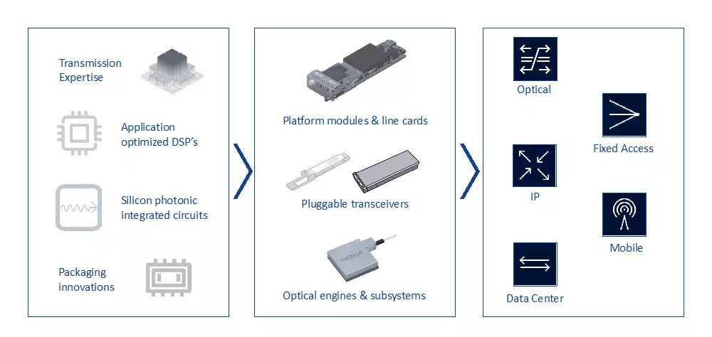
The WaveFabric Elements portfolio combines our PSE-V family of high-performance coherent DSPs with our innovative silicon photonics technology. It delivers fully integrated, end-to-end 400G coherent electro-optic solutions, including transceivers that are optimized for specific network applications. This high degree of vertical integration ensures that these solutions will meet the unique economic and technical requirements of data center, metro, long-haul, and subsea networks. With WaveFabric Elements, operators can deliver flexible and robust service experiences using new network architectures that apply the right technology for each application.
WaveFabric Elements also features a new family of pluggable transceiver modules. These modules address critical performance, cost, density and power requirements in data center, IP, and optical networks. They are also suitable for emerging markets and applications that are highly dependent on low-cost optical connectivity, such as access and mobile networking.
Preparing for the Terabit era
With each new generation, we achieve even higher levels of integration within our silicon photonics solutions. Increasing the percentage of the components required for photonic and electronic assemblies onto a silicon chip will help data center and network operators stay ahead of the demand curve with ever-improving economics. Moreover, our silicon photonics-based optics platform provides a foundation for integrating and scaling inter-chip connections for coherent electro-optics and on-board optics for chip-to-chip connections.
The next generation of silicon photonics solutions will support data rates of 800G and beyond. New co-packaging innovations and the integration of silicon photonics chips with coherent DSPs will enable the tight electrical-optical integration needed to operate at such data rates, and result in transport capabilities that further eliminate bandwidth and distance limitations. These innovations will significantly improve transmission performance, power efficiency, and density.
WaveFabric Elements: A portfolio to power the optical ecosystem

Our technology expertise, unique design platform and services enable us to address the critical and rapidly evolving optical connectivity requirements of 5G, cloud and enterprise networking. By combining these key assets with the massive scale and economies of silicon design and manufacturing, we help network operators keep up with new demands while reducing time to market, complexity and total cost of ownership.
Learn more
PSE Super Coherent Technology webpage
WaveFabric Elements webpage


