III-V Lab at the system core
Jointly operated by, Nokia, Thales and CEA, III-V Lab performs R&D on opto-electronic and micro-electronic components based on III-V semiconductor alloys. It realizes their integration with silicon circuits and micro-systems to cover markets addressed by the three parent companies.
The lab’s leading experts master the entire chain of design and implementation, starting with a deep understanding of physics at the atomic level. Working at the system core, they meet desired specifications by creating custom semiconductor materials that do not exist in nature.
This approach takes advantage of the commonalities among technologies developed for different markets, including telecom, space, defence and security. Examples include high-bit-rate optical fiber and wireless telecommunications, microwave and photonic systems for defence, security and aerospace.
Established in 2004 and located at the heart of the Paris-Saclay scientific campus, III-V Lab covers investigation from basic research to technology transfer for industrialization. It also has the capacity to produce and sell components (epitaxial wafers, processed wafers, modules) in small prototyping quantities. This approach fosters the emergence of high-added-value component technology that can then be transferred to the industrial entities of the parent companies or their partners.
Compound Semiconductor Epitaxy Research
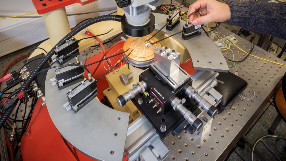
In-house components and circuits prototyping, from material research to devices to prototypes: Multi Physics Modelling, Material Growth (Epitaxy), Wafer Processing, Measurement
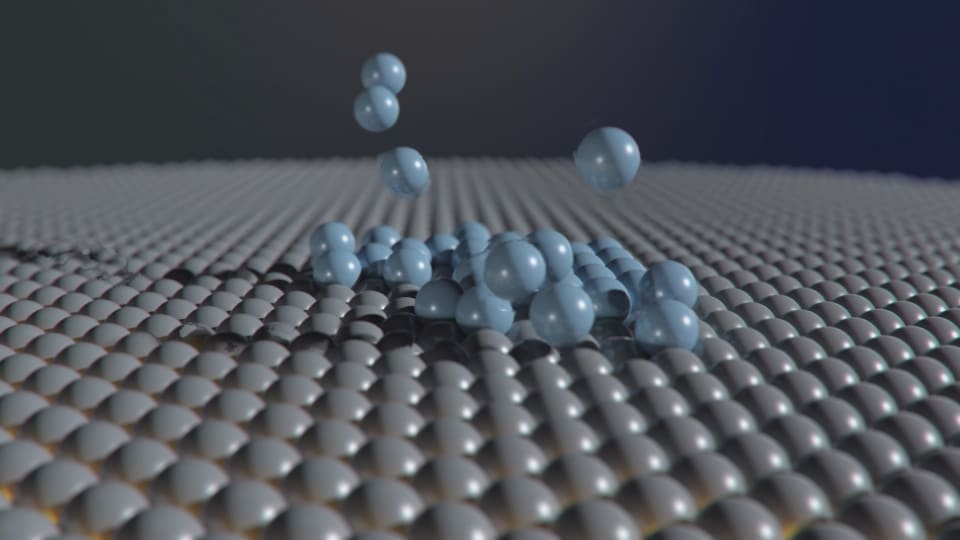
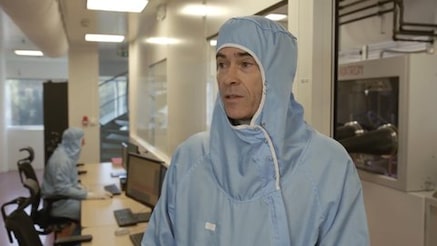
Mastering material at the atomic scale
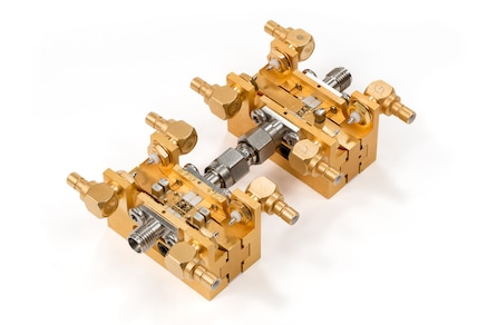
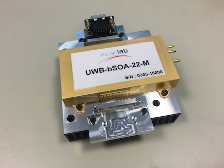
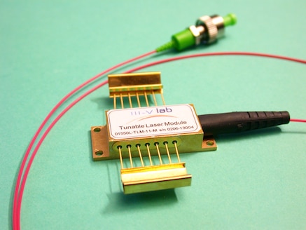
Some device realizations

Discover more

Video
AI-enhance wireless reliability: joint source and channel coding for robust 6G air interface

Blog

Blog

Podcast